- -$20.00
- Out-of-Stock


Our test shows that the sound from AD1865 SMT package is much better than it's DIP package. There are two clear advantages, 1)smaller SMT package size can achieve shorter decoupling distance from the capacitor, 2)Different pin arrangement of SMT package can give better PCB layout.
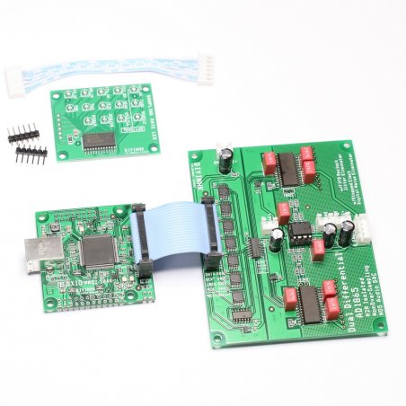
R2R, RECLOCK, ISOLATED, NONOVERSAMLING, all mystery area in the audiophile world are now included in an all-in-one compact PCB!
The I2S reclock input circuit in this PCB is based on the Analog Device AN207 stop clock algorithm, left and right channel DAC are latch at the same time. With our enhanced and optimized redesign, it has no phase different problem as the other convertor in the market. The MCK from the I2S input is used to drive the input flip flop for FIFO reclock, it do not have the problem as the other complex reclock scheme which drop or double dozens of unnecessary samples every second, and it do not use CPLD/FPGA as the other design which actually increase the jitter tenth of time after reclock. This PCB is target for audiophile.
The sound from this DAC is unique, sweet, clear and full of detail that the newest cutting edge delta sigma DAC can never produce. If you haven't taste this kind of sound before it's definitely a regret for an audiophile. It's like compare Vinyl and CD, Rollling shutter and global shutter in the DSLR.
This item includes PCB with all SMT component soldered, thru-hole component are not soldered.
Features:
1) Dual Dedicated AD1865 in full differential mode for each channel. (Not simply parallel the output of the same or different dac, differential mode is the better and more advance method)
2) AD1865R 110dB SNR 0.003% THD R2R DAC Chip (Optional)
3) Solid ground plane with careful split of digital and analog portion(a must for highest fidelity audio)
4) 0.1% Low noise thin film resistor and C0G Capacitor sourced from Digikey USA (guarantee no fake product from China)
5) Gold plate I2S input connector and four dedicated GND return path for each I2S signal(lowest contact resistance and highest signal quality)
6) The included xmos pcb in the combo is the same as the one sell separately in the store(i.e. flashed with general firmware)
User guide:
1)The AD1865R PCB can work immediately with only I2S signal and power supply connected, one 3.3V (>300mA) and one +-5V (>100mA).The +-5V power can be supplied by two individual 5V supply. i.e. 5V1 GND1, 5V2 GND2 connected as 5V=5V1, GND=GND1=5V2, -5V=GND2
2)The reclock quality depends on the jitter of MCK, When used with our XMOS PCB, the MCK is connected to the low jitter low phase noise NDK oscillator directly and achieve the best reclock performance.
3)For windows, set the output to full volume and the same sample rate as the music file for bit perfect non-oversampling NOS audio playback.
4)Microsoft acquires Pacific Microsonics(inventor of the renowned PMD100 and PMD200 digital filter) at Sep-2000, windows user should enjoy the same sound signature as using PMD100/200 when switch to listen at higher than the original music file sample rate from the system sound control panel using NOS DAC.
5)Double check all the capacitor are installed in the correct polarity before turn on your power supply.
6)For Diyer requires more deeper customization or customized IV stage, the Iout directly from the DAC chip is connected to a 2.54mm spacing socket. For advanced usage, the latest version of AD1865 datasheet is available in the official analog device website.
7)Tips only for option: DAC PCB without DAC chip. The thick solder on the AD1865R soldering pad is used for user easily to install the smt IC and it should not be removed normally.
The normal procedure to install the smt IC:
a) paint a thin layer of soldering flux on the top of the pad which already has thick solder
b) place the IC on the pad
c) use a hot air gun ~340C to blow it from 3-5cm distance. Do not blow it longer than 2min. the IC can be damaged.
d) while the solder melt, the IC should auto align to it's position(due to surface tension from the liquid stage of the solder) If it is still misaligned, user can use a tweezer to move the ic to it's position while the solder is still in the liquid stage. The finish quality of this method will be as good as a computer motherboard.
8)Compact size 80mm x 100mm
Specification:
1) I2S Input: MCK, LRCK, BCK, DATA (*BCK = 64x LRCK, MCK >= 2x BCK)
2) Output level: 2V RMS
3) Resolution/Sampling Rate: Upto 16,24,32bit / 192KHz (the most significant 18bit is played)
4) Supply: Regulated 3.3V, +-5V
*The included AD1865R DAC chip is new old stock or fully tested recycle chip with different batch number.
This item is in limited stock, maximum two per buyer. Please contact us if you want to buy more than two, thanks.
You might also like